


ABIDI Projects
Project Overview
ABIDI-I
.jpeg)
ABIDI-II
.jpeg)
On-Chip Inductor Based Step Down Converter with Fast Transient Response
In this work, our area of interest is focused on the design of fully integrated on-chip DC-DC step down converter with fast transient response. DC-DC Converters usually consist of power stage and control stage.
The power stage controls the efficiency of the converter. The power stage usually consists of switches, inductor, capacitor and load. Fig. 1 shows the circuit diagram of DC-DC step down converter. When switch S1 is on, inductor stored the energy and the output voltage becomes equal to input voltage. When switch S2 is on, the inductor is discharging through switch S2, which results in the lower voltage as compared to the input voltage.
The control stage usually consists of an error amplifier along with compensation circuit for stability of the system. The error signal is then compared with the saw-tooth signal to generated respective duty cycle. The control stage helps us to mitigate the under shoot and overshoot of the system as well as to achieve the fast transient response of the system.
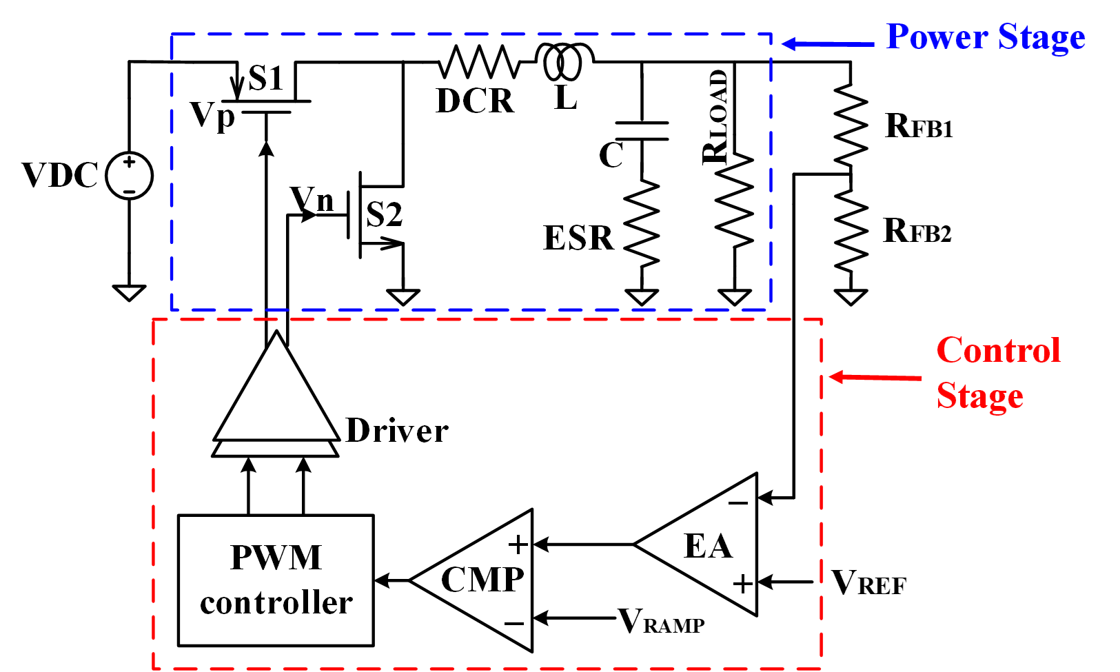
Fig. 1 Schematic of the conventional DC-DC step-down converter
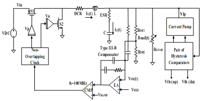
Fig. 2 Architecture of proposed monolithic voltage mode step down converter
Spatial Sigma-Delta ADC for Massive MIMO Applications
In this work, we proposed the complete module of spatial ∑Δ ADC consisting of modulator and digital low-pass filter (LPF). The digital output will be fed to the RISC-V Core. The proposed design is targeted for the 5G applications.
The proposed hardware implementation of spatial ∑Δ ADC for MMIMO utilizes a single-bit DAC, which yields high linearity. The proposed design consists of 4th order oversampling ∑Δ modulator. The proposed modulator block of the proposed ∑Δ ADC will be implemented on open source analog design tool, while the digital filter is modeled in MATLAB, and on chip implementation will be realized by open source digital design process flow in the SKY130 CMOS process.
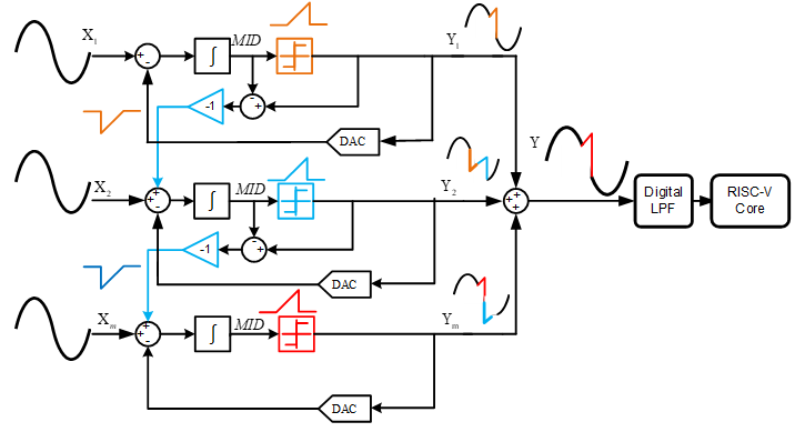
Fig.1 Block diagram of proposed architecture of spatial sigma-delta.
| Specifications | Target |
|---|---|
| Bandwidth | 2 MHz |
| Order | 4 |
| Signal to Noise and Distortion Ratio (SNDR) | Signal to Noise and Distortion Ratio (SNDR)> 55 dB |
| Over Sampling Ratio (OSR) | 40 |
| Active Area | < 1 mm2 |
Matrix Multiplier for AI on Edge Applications
This project presents the implementation of a parallel computation framework for energy-efficient and rapid matrix multiplication utilizing a systolic array algorithm. The systolic array employs processing elements (PEs) and yields accelerated results compared to conventional matrix multiplication methods.
To address the constraints of limited power and area in parallel computation, we have integrated the Modified Booth Wallace Multiplier as the core processing element. This multiplier incorporates modules such as the Booth encoder, partial product generator, Wallace tree formation, and a fast adder, such as the Carry Look Ahead Adder.
The Modified Booth algorithm significantly reduces partial products, offering a substantial area reduction for both Radix-4 and Radix-8 encodings. By combining the Modified Booth Wallace Multiplier with a Wallace tree structure, we aim to optimize both area utilization and processing speed, resulting in an efficient and rapid matrix multiplication process.
Fig. 1 Matrix multiplication using systolic array algorithm representation
Auto-Start Curvature Compensated CMOS Bandgap Reference
The proposed voltage reference circuit employs a curvature-compensated Bandgap Reference (BGR) architecture to address temperature-dependent variations in the output voltage. Unlike conventional BGRs, which exhibit non-linear temperature responses due to the dependence of the base to emitter voltage (VBE) on temperature, the proposed design incorporates a sophisticated compensation mechanism.
This involves extracting the silicon bandgap voltage at zero Kelvin (VG0) from the BJT VBE(T) equation, and compensating for both the complementary temperature coefficient (CTAT) and the non-linear terms using a three-diode connected model with self-bootstrapping. The resulting curvature-compensated BGR voltage (Vref) is achieved by combining the uncompensated bandgap reference voltage (Vo) with temperature-dependent terms (VPTAT and VNL).
This approach not only reduces the temperature coefficient but also improves power supply rejection ratio (PSRR), ensures auto start-up during supply voltage transients.
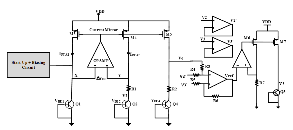
Fig 1. VGO extractor based on conventional BGR circuit
Self-Interference Cancellation Low Noise Amplifier for 5G and beyond
In addressing the challenges associated with Self-Interference (SI) in In-Band Full-Duplex (IBFD) radios, the proposed solution focuses on enhancing the design of a wideband Low Noise Amplifier (LNA) for 5G systems. Emphasizing the importance of maintaining low Noise Figure (NF) and high gain in the first stage of the receiver chain, the design incorporates an inductor-less architecture, wide bandwidth, and linearity.
Inspired by previous works, the proposed LNA comprises a Common-Source stage (M1), a Cascode stage (M4) for high gain, a current reuse device (M5) for gain with low power consumption, and a Common-Drain stage (M2) for partial noise cancellation. Building on advancements from prior research, two additional devices (M11 and M12) are introduced at distinct nodes of the LNA to mitigate SI.
Functioning as current sources, M11 and M12 inject anti-SI signals at nodes "1" and "2," leveraging Kirchhoffs Current Law to subtract SI within the LNA in current form. This innovative approach aims to effectively suppress SI without compromising the overall NF and gain of the receiver chain, providing a robust solution for IBFD radio implementations in 5G systems.
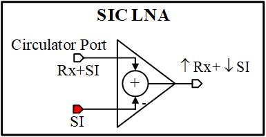
Fig 1. Block Diagram of Proposed LNA
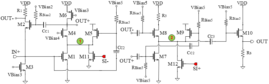
Fig 2. Schematic diagram of Half circuit of proposed Differential LNA
Encrypted LSB Steganography Implementation with AES-128 Accelerator
Various techniques are utilized today to secure sensitive data from unwanted access; the most effective are encryption and steganography. Steganography deals with concealing confidential information inside non-secret information using a mask to make it non-distinguishable. AES-128 is one of the most popular and strongest encryption ciphers in use nowadays.
Dedicated hardware implementations of these techniques provide more security and higher performance compared to software implementations. In this proposal, we propose a high-speed hardware architecture for the implementation of a combined unit for AES and Steganography of standard 128-bit input data.
The proposed architecture implementation on 130 nm pdk provides throughput higher than 800Mbps and power consumption of less than 10mW. Moreover, the proposed architecture achieves NIST compliant accuracy. The AES algorithm is implemented using a tradeoff is for maximum power, area efficiency and throughput.
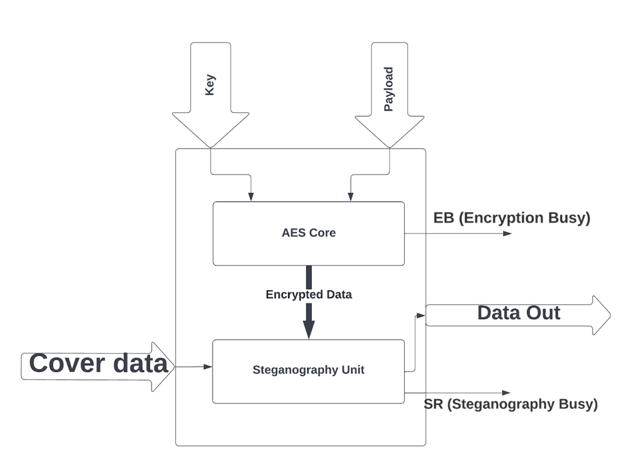
Fig 1. Proposed Architecture for IP